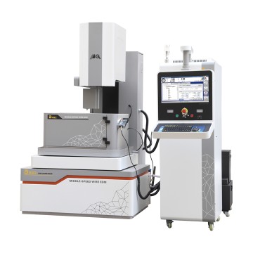
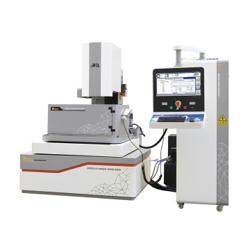
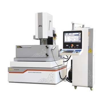
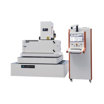
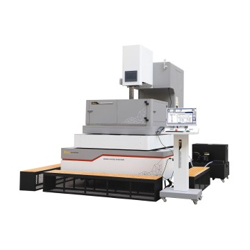
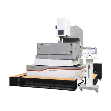
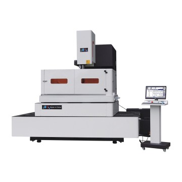
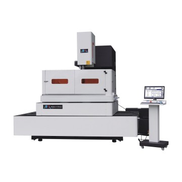
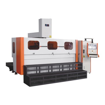
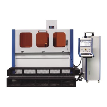
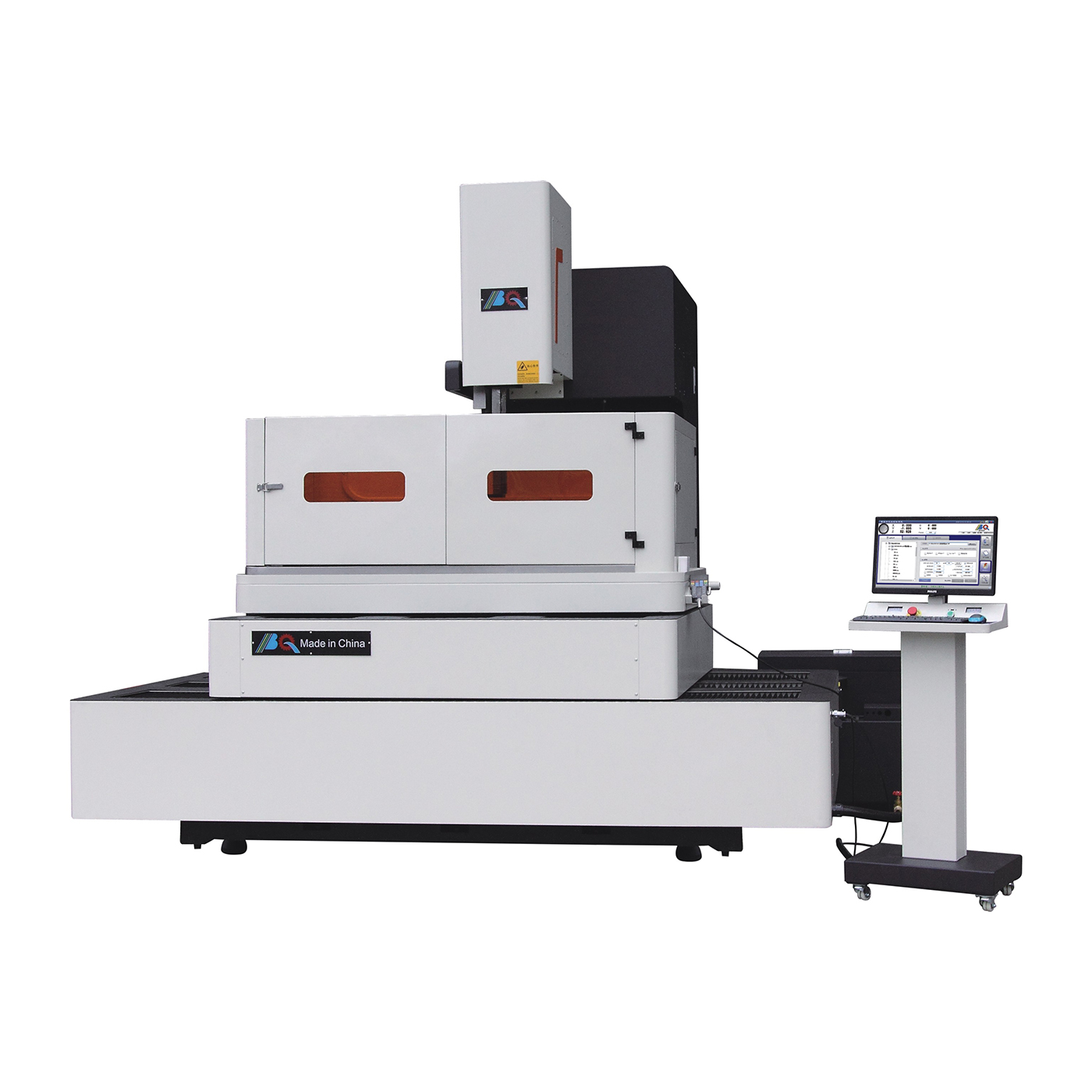
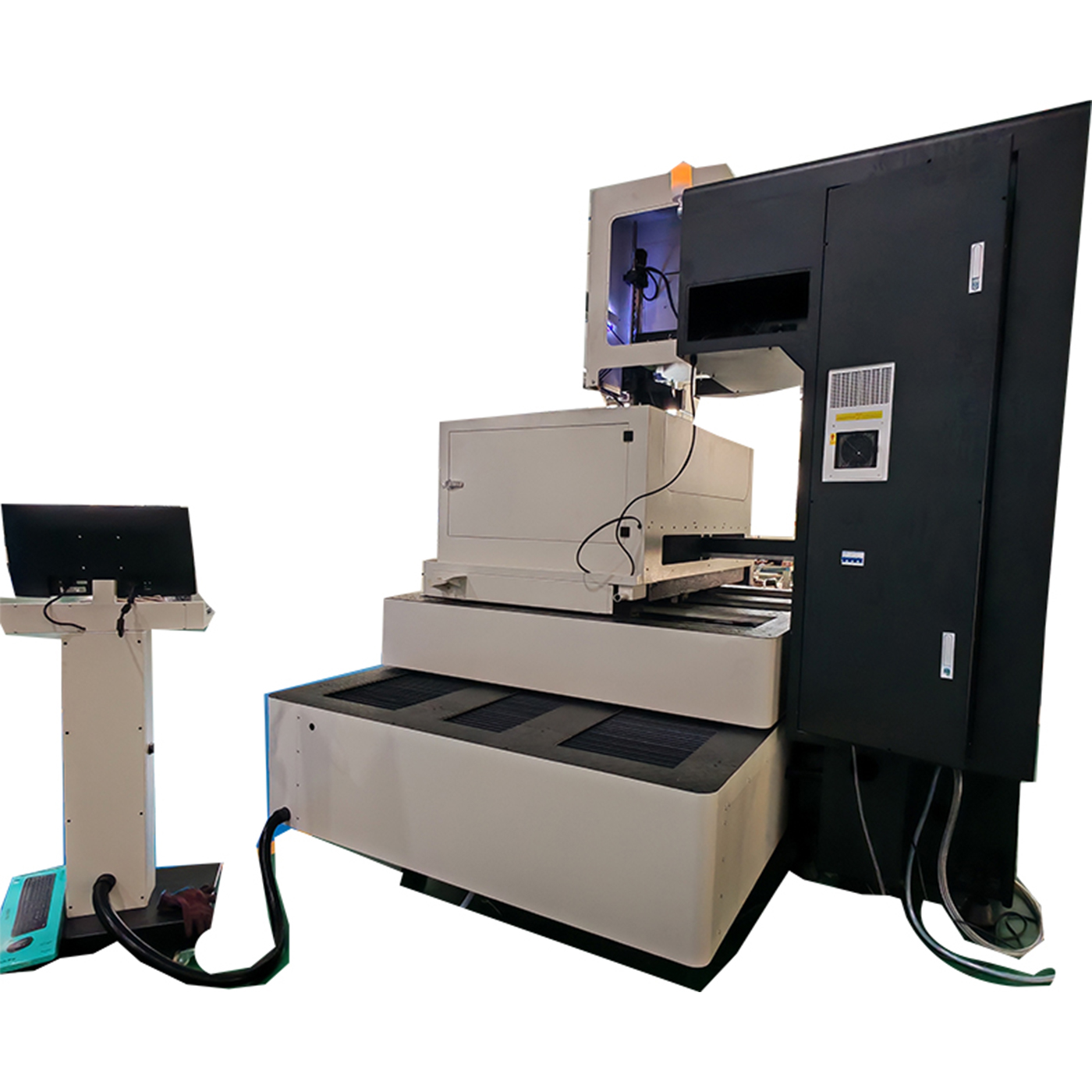
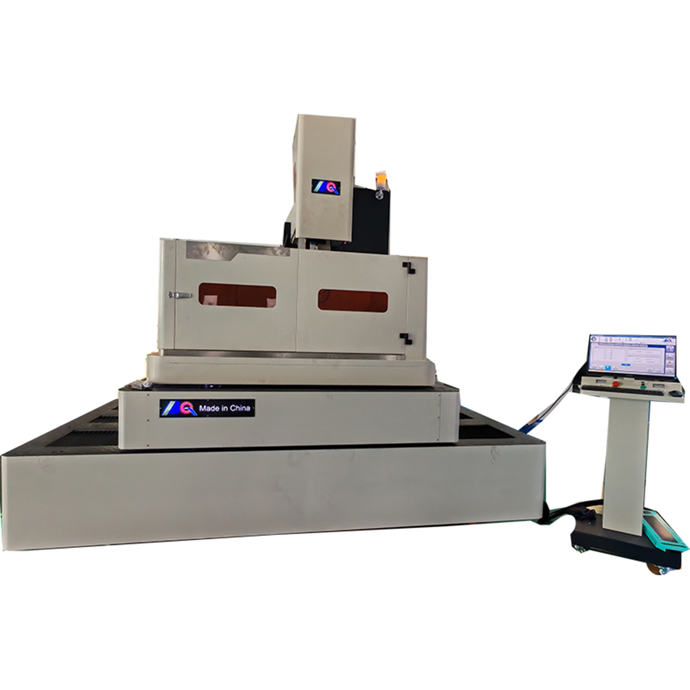
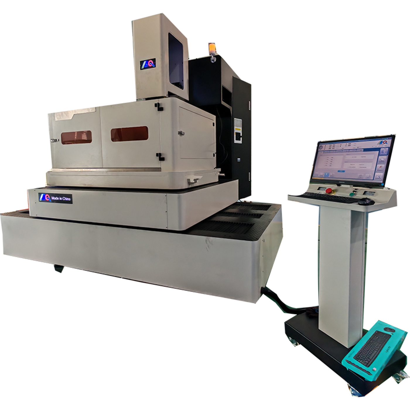
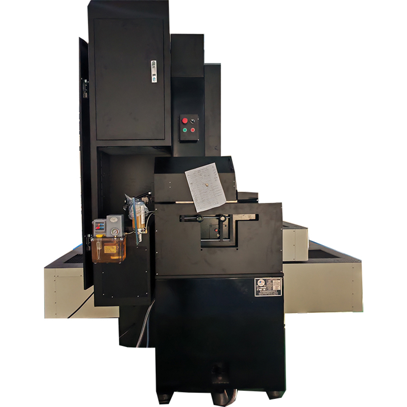
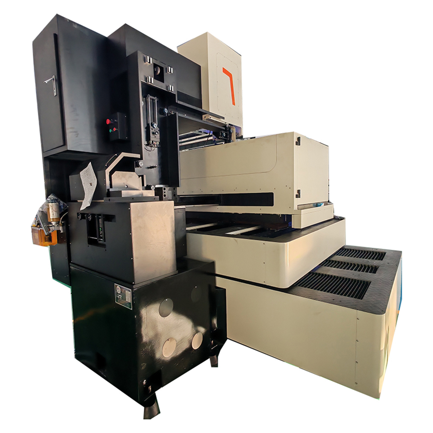
High Precision 5 Axis linkage BQ1080 Medium-Speed CNC Wire cutting EDM Machine
Share to:


Model |
BQ1080 |
|
Table travel |
Worktable size(mm) |
1360×970 |
X/Y travel (mm) |
1000×800 |
|
Max work piece size(mm) |
1600×1020 |
|
Max cutting thickness (mm) |
500 |
|
Max load weight (kg) |
2000 |
|
X/Y min.directive unit(mm) |
0.001 |
|
Taper and Z-axis travel |
Taper U/V travel (mm) |
80×80 |
Max cutting taper (mm) |
±15°/150 mm |
|
U/V min.command unit(mm) |
0.001 |
|
Transmission control |
Control method |
X/Y/U/V/Z Servo driven(Linear motor are option for X/Y) |
Z axis drive |
Numerical control |
|
Simultaneously controlled axes |
X Y U V-4 Axis |
|
Wire drum |
Max travel of wire drum(mm) |
200 |
Wire diameter(mm) |
①0.1-Φ0.2 (Standard 0.18) |
|
Wire speed(m/s) |
1-11.4 variable frequency |
|
Max.wire storage length (m) |
330 |
|
Machining parameters |
Reposition accuracy(mm) |
≤±0.003 |
Max cutting efficiency(mm²/min) |
≥300 |
|
Roughness/Ra(μm)cut 1 trim 2 |
0.7-1.4 |
|
Working liquid tank |
Liquid tank capacity |
130L |
Filtering method |
3 Layer filtration |
|
Others |
Power supply |
Three phase 380V AC/5OHz |
Control System |
Baqi system |
|
Total power consumption (kw) |
2.5 |
|
Max machining current(A) |
10 |
|
Machine gross weight(kg) |
8300 |
|
Machine size(mm) |
3140x2585×2980 |
|
Machine noise |
≤70dB |
|
Top-bottom irregular cutting |
Yes |
Baqi Intelligent's Medium-Speed Molybdenum Wire EDM are widely used in various fields such as mold and tooling, medical industry, aerospace, automotive parts, machining, military defense, and more. Let's explore the application characteristics and advantages of medium-speed wire cutting machines in different industries:
Applications and Advantages of Medium-Speed Molybdenum Wire EDM Machines in the Electronics/Semiconductor Industry
Medium-speed molybdenum wire EDM (medium-speed wire EDM) features medium-speed bidirectional wire feeding, multiple cuts, micron-level precision, and stress-free processing as its core characteristics. It perfectly meets the extreme demands of the electronics and semiconductor industries for miniaturization, high precision, high hardness, complex structures, and low stress. It is widely used in key processes such as semiconductor packaging, 5G communication, optoelectronics, and precision electronic component manufacturing, becoming a core precision machining solution balancing precision, efficiency, and cost.
Core Application Scenarios in the Electronics/Semiconductor Industry
1. Semiconductor Packaging and Heat Dissipation Component Processing
● Molybdenum-copper/tungsten-copper alloy heat sink substrate: Molybdenum-copper heat sink substrates, heat sinks, and packaging shells for high-power chips such as CPUs, GPUs, and IGBTs. This type of material has high hardness, strong thermal conductivity, and a thermal expansion coefficient that matches silicon wafers. Traditional cutting methods easily result in chipping and tool wear. Medium-speed wire EDM allows for stress-free precision cutting, forming complex shapes and micro-channels with dimensional accuracy of ±0.003mm and surface roughness Ra0.8μm.
● Leadframes and Packaging Molds: Processing semiconductor leadframes, IC packaging molds, and molding inserts. For 0.1~0.3mm ultra-thin copper alloy/nickel alloy materials, it achieves one-time forming of micro-narrow slits (0.08mm), micro-leads, and high-density leads, without burrs or deformation, meeting the lifespan and precision requirements of million-level packaging molds.
● Ceramic Metallized Substrate Etching: Processing metallized electrode grooves and positioning holes for semiconductor ceramic substrates, adapting to conductive ceramics such as alumina and aluminum nitride, solving the problem of easy breakage in traditional processing.
2. Precision Machining of 5G Communication and RF Devices
● RF Filter Cavities: Processing 5G base station metal cavity filters, resonant rods, and coupling plates. Workpieces are mostly thin-walled aluminum/copper alloy parts (wall thickness 0.3~0.8mm), processed with medium-speed wire EDM without cutting force, deformation controlled within 0.02mm, ensuring the accuracy of cavity resonant frequency.
● Microwave Circuit Components: Cutting waveguide components, microwave switches, and antenna elements to achieve complex structures with ±30° large taper, irregular shapes, and multi-step structures, ensuring stable electrical performance.
3. Precision Parts for Optoelectronics and Consumer Electronics
● Camera module bracket: Metal brackets for mobile phone/automotive lenses, focusing rings, and light shields. Processing coaxiality ≤0.003mm, micro-holes (φ0.1mm), and ultra-thin wall thickness (0.2mm), with no scratches and no stress on the surface.
● Miniature connectors and terminals: Processing PIN pins, contact springs, and miniature relay contacts with narrow kerf (0.05mm), high precision, and stable batch production to meet the consistency requirements of millions of units produced.
● High-density PCB: Cutting multi-layer PCBs, thick copper foil boards, flexible circuit board reinforcement boards, processing micro-vias, irregular grooves, and fine shapes, avoiding burrs and delamination problems of traditional milling.
4. Semiconductor Manufacturing Molds and Tooling Fixtures
● Wafer cutting blade molds, probe card fixtures, testing sockets: Processing precision fixtures made of hard alloy and stainless steel, with stable dimensions, wear resistance, and no stress, ensuring the positioning accuracy of semiconductor testing and packaging.
Core Advantages and Features (adapted to the Electronics/semiconductor Industry)
1. Stress Free Processing, Suitable for Ultra-Thin/deformable Electronic Materials
Non-contact electrical discharge machining (EDM), without mechanical cutting force, perfectly solves the deformation, warping, vibration marks, and chipping problems of ultra-thin copper/aluminum/molybdenum alloys (0.1~0.5mm) and microstructures in traditional cutting. When machining φ0.1mm micro-holes and 0.08mm narrow slits, the form and position tolerances are controllable and burr-free, directly meeting electronic assembly standards.
2. Ultra Precision Machining Capability to Meet Semiconductor Micron Level Requirements
Multiple cutting processes (roughing → finishing → smoothing) achieve dimensional accuracy of ±0.003~±0.005mm and surface roughness Ra0.5~1.2μm, approaching the level of slow wire EDM. φ0.1~0.2mm ultrafine molybdenum wire can be used to achieve micro-contour, micro-radius (R0.01mm), and high-precision hole machining, adapting to the trend of semiconductor miniaturization and high-density integration.
3. Suitable for High Hardness/special Conductive Materials
Can process any conductive material without hardness limitations: molybdenum copper, tungsten copper, hard alloys, stainless steel, nickel alloys, conductive ceramics. Compared to traditional cutting, there is no tool wear, resulting in a 50% increase in efficiency and a 40% reduction in cost for processing high hardness electronic materials.
4. High Cost-Effectiveness, Balancing Production Efficiency and Cost
● Efficiency: Roughing efficiency 80~150mm²/min, overall efficiency is 30%~50% better than slow wire EDM.
● Cost: The equipment price is 1/3 to 1/2 of that of slow-moving wire, and molybdenum wire can be used repeatedly (the cost of consumables is only 1/5 of that of slow-moving wire and copper wire), resulting in low operation and maintenance costs. Suitable for the flexible production needs of small batches, multiple varieties, and rapid changeover in the electronics industry.
5. Ability to Process Micro and Complex Structures
Multi-axis linkage, upper and lower irregular shapes, large taper (±30°) cutting, one-time forming of 3D curved surfaces, inclined holes, and variable cross-section electronic components. Narrow kerf (0.05~0.12mm), high material utilization, suitable for processing electronic parts of precious metals and rare alloys.
6. Intelligent CNC, Adapted to the High Stability Requirements of the Electronics Industry
Adaptive pulse power supply: Automatically matches materials and thicknesses, optimizes discharge parameters, reduces wire breakage, and ensures batch stability. Micron-level closed-loop control (grating ruler + servo drive) achieves a repeatability accuracy of ≤±0.003mm, meeting the consistency requirements of million-level mass production.
Comparison Between Medium Speed Wire and Slow/fast Speed Wire in the Electronics Industry
Performance dimension |
Medium speed molybdenum wire (medium speed wire) |
Wire-cut EDM |
Hurry up, silk |
precision |
±0.003~±0.005mm |
±0.001~±0.003mm |
±0.02~±0.05mm |
Surface quality |
Ra0.5~1.2μm |
Ra0.2~0.8μm |
Ra3.2~6.3μm |
Microfabrication |
φ0.1mm thread, 0.08mm seam |
φ0.05mm thread, 0.03mm seam |
φ0.18mm thread, 0.15mm seam |
efficiency |
High (considering both coarse and fine) |
Low (slow refinement) |
High (only thick) |
cost |
Medium (with the highest cost-effectiveness) |
extremely high |
low |
Electronic/semiconductor adaptation |
★★★★★ |
★★★★☆ |
★★☆☆☆ |
Summary
In the trend of miniaturization, high frequency, high power, and high-density integration in the electronics and semiconductor industries, medium-speed molybdenum wire EDM machines, with their comprehensive advantages of stress-free operation, high precision, high material adaptability, and high cost-effectiveness, have become the preferred process for precision parts processing in semiconductor packaging, 5G communication, optoelectronics, and consumer electronics. It meets the stringent processing standards for ultra-thin, micro-fine, and high-hardness electronic parts while significantly reducing equipment and production costs and improving processing efficiency, perfectly balancing quality, efficiency, and cost. It is an indispensable "precision embroidery needle" in the electronics manufacturing field. With the continuous upgrading of semiconductor and electronic technologies, the iteration of medium-speed wire EDM in the directions of ultra-fine, intelligent control, and automated integration will further expand its application boundaries in high-end electronics manufacturing.
Product advantages and applicable industries
-
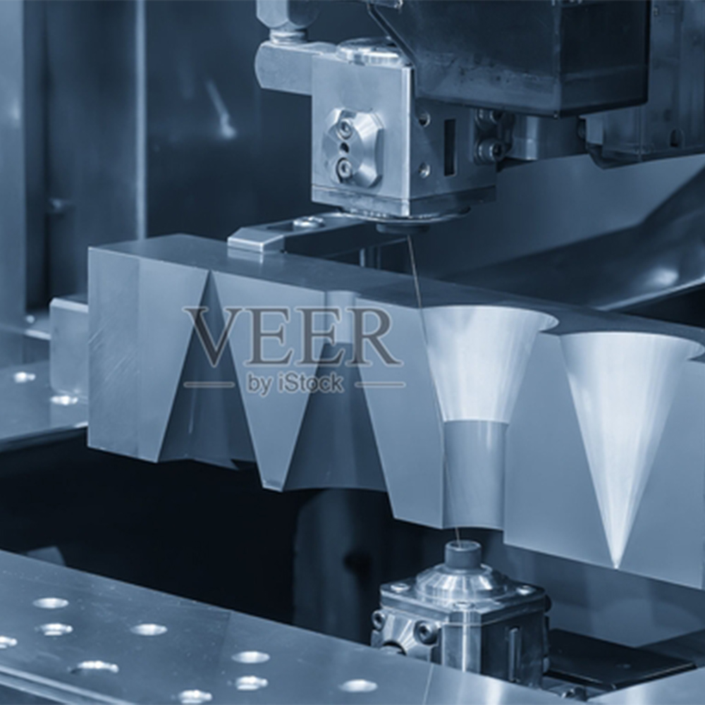
Wire cutting machine tool processing stamping die on site
-
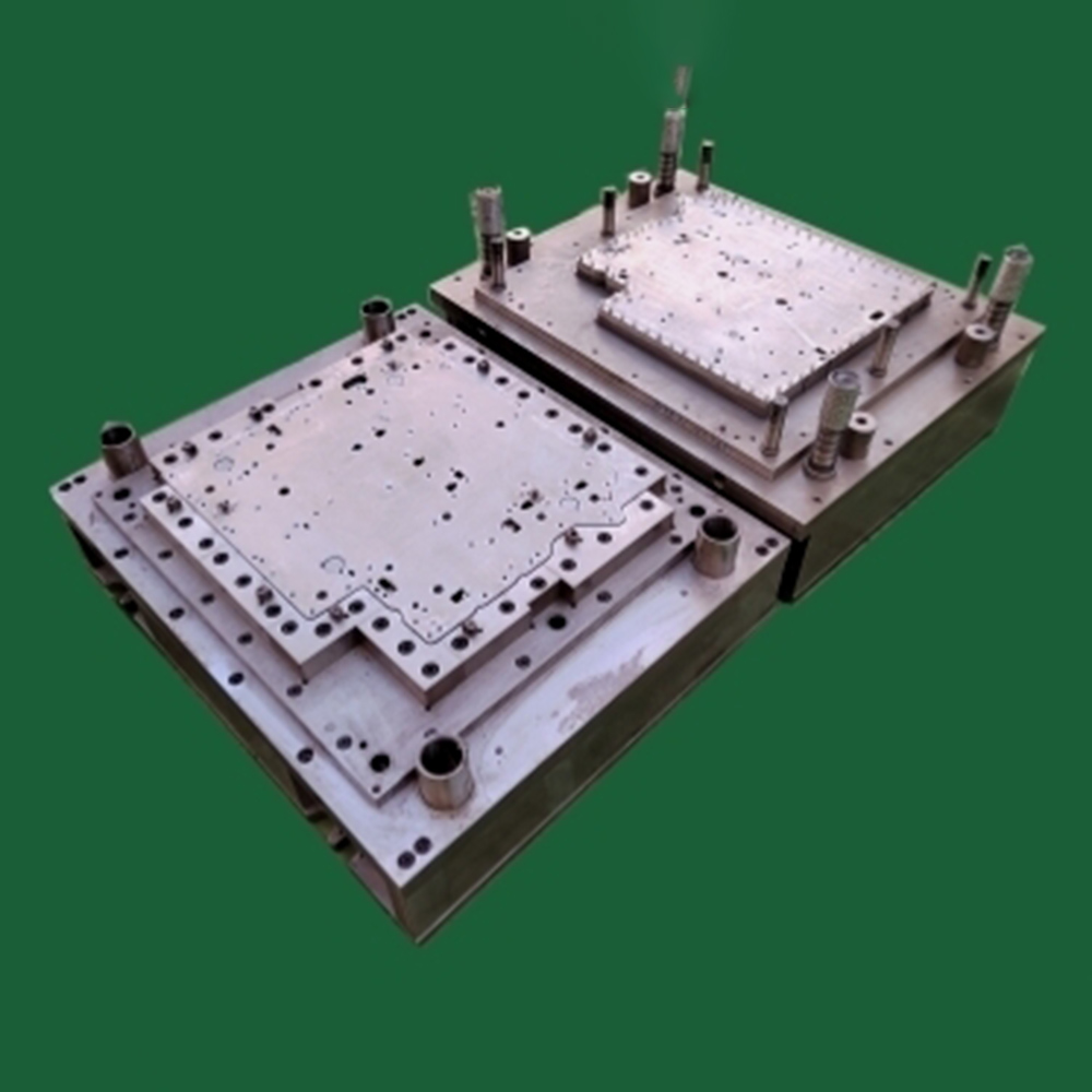
Multi-station continuous stamping die (integrated wire cutting)
-
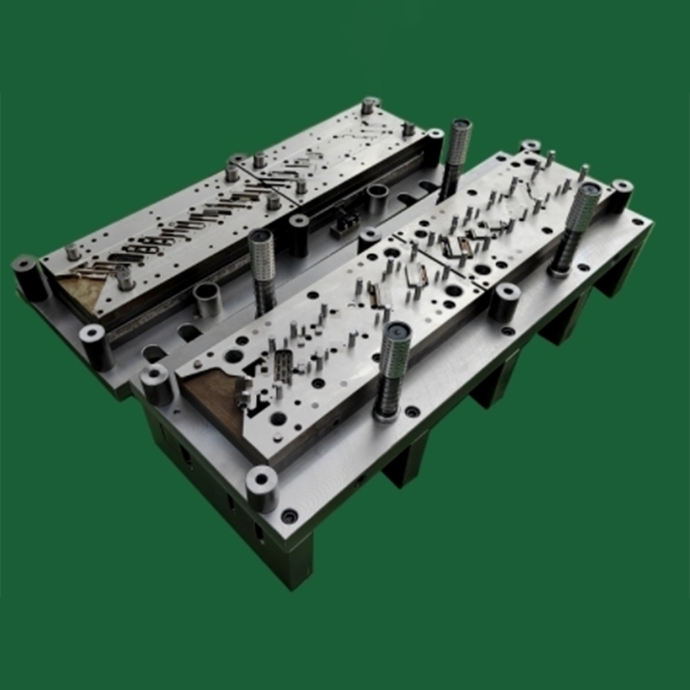
terminal progressive die (typical product of wire cutting)
-
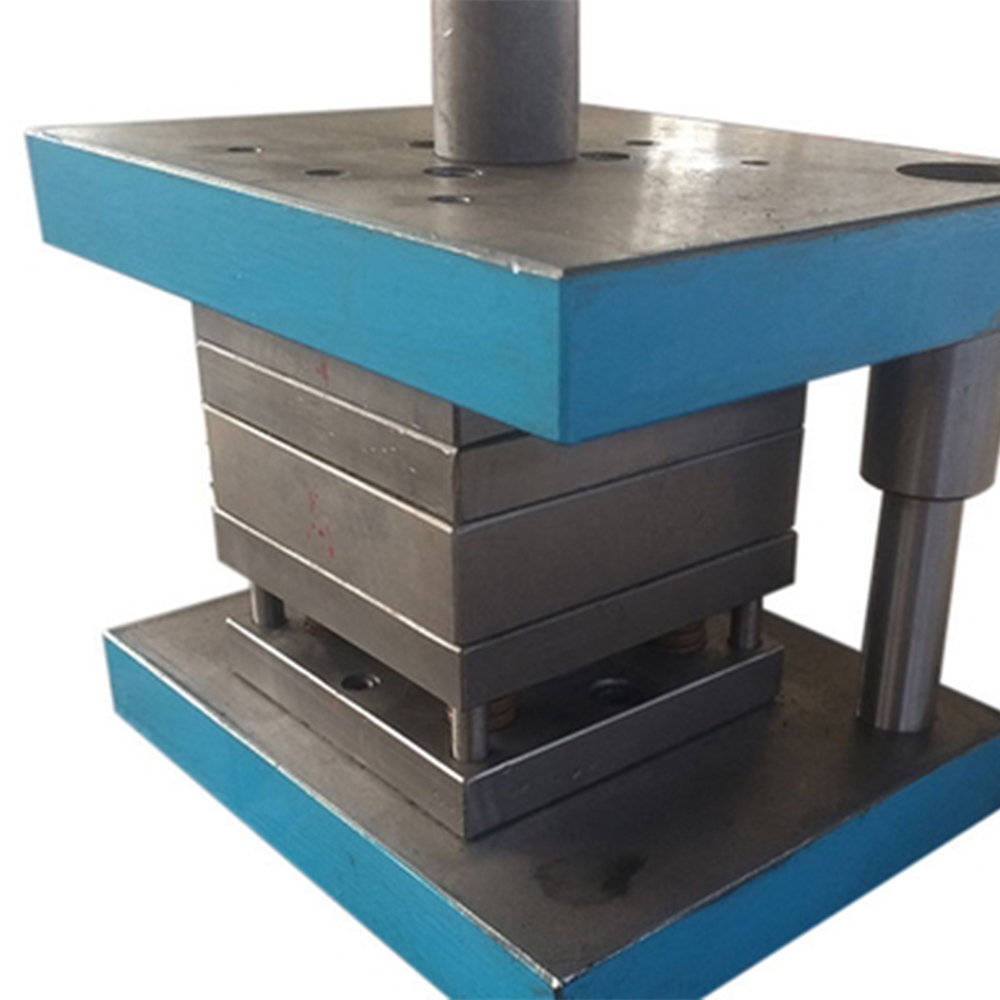
Motor silicon steel sheets, stator and rotor stamping molds (areas where wire cutting excels)